ZigBee module introduction–TYZS3-IPEX
1. Product overview
The TYZS3-IPEX is a low-power, embedded Zigbee module developed by Hangzhou Tuya Information Technology Co., Ltd. The module consists of a EFR32MG13P732 highly integrated wireless RF processor chip and a small number of peripheral devices. It has a built-in 802.15.4 PHY/MAC Zigbee network protocol and a large number of library functions. The TYZS3-IPEX embeds a low-power 32-bit ARM Cortex-M4 core, 512KByte Flash program memory, 64KB RAM data memory, and a wealth of peripheral resources.
The TYZS3-IPEX is a FreeRTOS platform that gathers all Zigbee MAC and TCP/IP libraries into one place. It enables users to build on the product and develop embedded Zigbee products that suit their individual needs.
The TYZS3-IPEX schematic diagram as shown in Figure 1:

1.1 Features
A built-in low-power 32-bit ARM Cortex-M4 processor with a DSP instruction set and a floating point unit that doubles as an application processor
- Supports a main frequency of 40MHz
Wide operating voltage: 1.8V-3.8V
Peripherals: 9×GPIOs, 1×UART, 1×ADC
Zigbee operating characteristics
- Supports 802.15.4 MAC/PHY
- Operating channels 11 to 26 @2.400-2.483GHz, air-interface rate 250Kbps
- Built-in DC-DC circuit for maximum power efficiency
- +19dBm maximum output, dynamic power output > 35dB
- 63uA/MHz operating power consumption; 1.4 uA sleep current
- Active net pairing with terminal devices
- Built-in onboard PCB antenna/reserved Ipex connector for high gain external antenna
- Operating temperature: -40℃ to 85℃
- Supports hardware encryption and supports AES 128/256
1.2 Primary application fields
- Smart buildings
- Smart homes/appliances
- Smart plugs, smart lighting
- Industrial wireless control
- Health and measurements
- Asset tracking
2. Module interfaces
2.1 Package dimensions
The TYZS3-IPEX has 2 rows of pins with a 2mm gap.
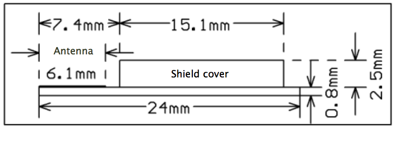
TYZS3-IPEX dimensions: 16mm (W) x 24mm (L) x 3.5mm (H). The TYZS3-IPEX’s dimensions are shown in Figure 2:


2.2. Pin definition
Interface pins are defined as shown in Table 1:
Table 1, TYZS3-IPEX interface pins description
| Pin number | Symbol | IO Type | Function |
|---|---|---|---|
| 1 | nRST | I | Hardware reset pin, the chip is reset when the pin is LOW; Power-on reset of the module, the user can use this pin as needed |
| 2 | ADC | AI | ADC, 12-bit precision SAR analog to digital converter |
| 3 | NC | - | NC pin, external handling is not required |
| 4 | GPIO0 | I/O | GPIO pin usage. |
| 5 | SWO | I/O | GPIO pin usage/can be used as an output pin under JLINK communication. |
| 6 | PWM3 | I/O | GPIO pin usage. |
| 7 | PWM1 | I/O | GPIO pin usage. |
| 8 | VCC | P | Module power supply pin (common supply voltage: 3.3V) |
| 9 | GND | P | The reference ground of the module. |
| 10 | GPIO2 | I/O | GPIO pin usage. |
| 11 | SWDIO | I/O | JLINK SWDIO programming pin. Can be used as a GPIO pin in normal applications. |
| 12 | SWCLK | I/O | JLINK SWCLK programming pin. Can be used as a GPIO pin in normal applications. |
| 13 | PWM2 | I/O | GPIO pin usage. |
| 14 | GPIO3 | I/O | GPIO pin usage. |
| 15 | RXD | I/O | UART0_RXD |
| 16 | TXD | O | UART0_TXD |
Description: P indicates the power pin; I/O indicates the input/output pin; AI indicates analog input pin.
nRST is only the module hardware reset pin; it cannot clear Zigbee net-pairing information.
(1): This pin can only be used as an ADC port. It cannot be used as a normal IO port. If it is not used, it needs to be left floating.
As an ADC input, the input voltage range is limited to 0-AVDD and can be configured by software.
2.3 Test point definition
Test pins are defined in Table 2:
Table 2, TYZS3-IPEX test pins description
| Pin number | Symbol | IO Type | Function |
|---|---|---|---|
| - | - | I | For module production testing |
Description: This test pin is not recommended for use.
3. Electrical parameters
3.1 Absolute electrical parameters
Table 3, Absolute parameters
| Parameters | Description | Minimum value | Maximum value | Unit |
|---|---|---|---|---|
| Ts | Storage temperature | -50 | 150 | ℃ |
| VCC | Input voltage | -0.3 | 3.8 | V |
| Electrostatic discharge voltage (human-body model) | TAMB-25℃ | - | 2.5 | KV |
| Electrostatic discharge voltage (machine model) | TAMB-25℃ | - | 0.5 | KV |
3.2. Operating conditions
Table 4, Normal operating conditions
| Parameters | Description | Minimum value | Typical value | Maximum value | Unit |
|---|---|---|---|---|---|
| Ta | Operating temperature | -40 | - | 85 | ℃ |
| VCC | Operating voltage | 1.8 | 3.3 | 3.8 | V |
| VIL | IO low input | -0.3 | - | VCC*0.25 | V |
| VIH | IO high input | VCC*0.75 | - | VCC | V |
| VOL | IO low output | - | - | VCC*0.1 | V |
| VOH | IO high output | VCC*0.8 | - | VCC | V |
| Imax | IO drive current | - | - | 12 | mA |
3.3 Zigbee TX power consumption
Table 5, Power consumption during continuous TX
| Symbol | Rate | Transmission power | Typical value | Unit |
|---|---|---|---|---|
| IRF | 250Kbps | +19dBm | 120 | mA |
| IRF | 250Kbps | +13dBm | 50 | mA |
| IRF | 250Kbps | +10dBm | 32 | mA |
| IRF | 250Kbps | +4dBm | 17 | mA |
| IRF | 250Kbps | +1dBm | 11.8 | mA |
Note: When testing the above data, the continuous transmission duty cycle=100%.
3.4 Zigbee RX power consumption
Table 6, Power consumption during continuous RX
| Symbol | Rate | Typical value | Unit |
|---|---|---|---|
| IRF | 250Kbps | 8 | mA |
Note: When UART is active, the RX current is 14mA.
3.5 Power consumption in operating mode
Table 7, TYZS3-IPEX operating current
| Operation mode | Operating condition, Ta=25℃ | Average value | Maximum value | Unit |
|---|---|---|---|---|
| Quick configuration | Module in quick configuration state | 10 | 40 | mA |
| Network connection state | Connected to a network | - | - | mA |
| Deep sleep mode | Deep sleep mode and retains 64KB Flash | 1.4 | 3 | uA |
4. RF Characteristics
4.1 Basic RF characteristics
Table 8, Basic RF characteristics
| Parameter | Description |
|---|---|
| Operating frequency | 2.400 to 2.484GHz |
| Physical layer standard | IEEE 802.15.4 |
| Data transfer rate | 250Kbps |
| Antenna type | Ipex connector external antenna |
| Line of sight transmission distance | 200m (10dBm transmit power) |
4.2 Zigbee Output performance
Table 9, ContinuousTX performance
| Parameter | Minimum value | Typical value | Maximum value | Unit |
|---|---|---|---|---|
| Maximum output | - | +19 | - | dBm |
| Minimum output | - | -30 | - | dBm |
| Output power adjustment step | - | 0.5 | 1 | dB |
| Frequency error | -15 | - | +15 | ppm |
| Output adjacent channel suppression | -31 | dBc |
Note: The maximum output power is +19dBm. The power output can be adjusted under normal use. The high-power output can be used for overlay transmissions in extremely complex environments, such as modules embedded in the wall.
4.3 Zigbee RX sensitivity
Table 10, RX sensitivity
| Parameter | Minimum value | Typical value | Maximum value | Unit |
|---|---|---|---|---|
| PER<10%, RX sensitivity, 250Kbps@OQPSK | -102 | -101 | -99 | dBm |
5. Antenna signal
5.1 Antenna type
An external antenna can be connected via the Ipex connector for extended coverage in complex installation environments.
5.2 Antenna interference reduction
To optimize Zigbee performance of the wireless module in combination with the PCB onboard antenna, it is recommended to keep the antenna at least 15mm from other metal parts. It is recommended that the corresponding antenna area of the adapter board be hollowed out for the best effect.
The user PCB board should not be routed around the antenna area and should not be covered with copper to avoid affecting the antenna radiation performance.
For the module PCB onboard antenna area, refer to Figure 3 “TYZS3-IPEX mechanical dimensional drawing” below.
6. Packaging information and production guidance
6.1 Mechanical dimensions

6.2 PCB recommended packaging


6.3 Production guide
The storage conditions for the module after it has been shipped are as follows:
1. The moisture resistant bag must be stored at a temperature below 30℃, and under a relative humidity below 85%.
2. The shelf life of dry packed products is 6 months following the packaged date.
Important information
1. All line workers must wear anti-static wrist straps and anti-static clothing throughout the entire production process.
2. It is strictly prohibited to allow a module to come into contact with water or other contaminants during operations.
6.4 Recommended furnace temperature curve

TYZS3-IPEX Data Sheet
- 1. Product overview
- 1.1 Features
- 1.2 Primary application fields
- 2. Module interfaces
- 2.1 Package dimensions
- 2.2. Pin definition
- 2.3 Test point definition
- 3. Electrical parameters
- 3.1 Absolute electrical parameters
- 3.2. Operating conditions
- 3.3 Zigbee TX power consumption
- 3.4 Zigbee RX power consumption
- 3.5 Power consumption in operating mode
- 4. RF Characteristics
- 4.1 Basic RF characteristics
- 4.2 Zigbee Output performance
- 4.3 Zigbee RX sensitivity
- 5. Antenna signal
- 5.1 Antenna type
- 5.2 Antenna interference reduction
- 6. Packaging information and production guidance
- 6.1 Mechanical dimensions
- 6.2 PCB recommended packaging
- 6.3 Production guide
- 6.4 Recommended furnace temperature curve