title: TYWE3S Module
subtitle: WiFi module module TYWE3S datasheet specification
published: true
–
WiFi module introduction–TYWE3S
1. Product Overview
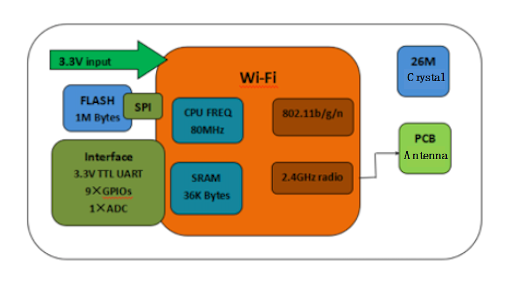
TYWE3S is a low-power embedded Wi-Fi module developed by Hangzhou Tuya technology co., LTD. It consists of a highly integrated radio frequency chip ESP8266 and a handful of peripheral components, with a built-in Wi-Fi network protocol stack and rich library functions. TYWE3S is built in low-power 32-bit CPU, 2Mbyte flash memory, 50KB SRAM and rich peripheral resources.
TYWE3S is a RTOS platform that integrates all Wi-Fi MAC and TCP/IP protocol libraries. Users can develop embedded Wi-Fi products that meet their needs based on these developments.
The functional diagram of TYWE3S is shown in Figure 1:
1.1 Features
- Built-in low-power 32-bit CPU, can be concurrently used as an application processor (main-frequency support 80MHz & 160MHz)
- Built-in low-power 32-bit CPU can be concurrently used as an application processor (main-frequency support 80MHz and 160MHz)
- Working voltage:3V-3.6V
- Peripheral:9×GPIOs, 1×UART, 1×ADC
- Wi-Fi connectivity
- 802.11b/g/n
- Channel 1-14@2.4GHz
- Support WPA/WPA2 safe mode
- 802.11b mode + 20dBm output power
- Support STA/AP/STA+AP work mode
- Support SmartConfig function(including Android & iOS devices)
- Onboard PCB antenna
- Working temperature:-20℃-85℃
1.2 Major application fields
- Smart building
- Smart home appliances, smart home
- Smart plug. smart lighting
- Industrial wireless control
- Baby monitor
- Webcam
- Smart bus, etc
2. Dimensions and Footprint
2.1 Dimensions
TYWE3S has 2 rows of pins, lead pitch is 2mm.
TYWE3S size dimension:16±0.3mm (W)×24±0.3mm (L) ×3.4±0.2mm (H) 。
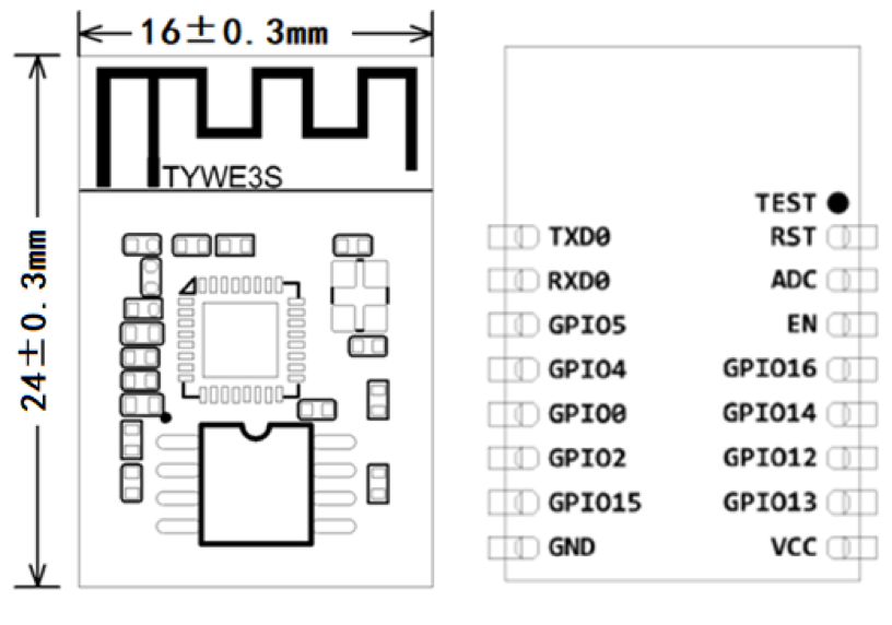 Figure 2. TYWE3S front and back view
Figure 2. TYWE3S front and back view2.2 Definition of pin
| 引脚序号 | 符号 | IO 类型 | 功能 |
|---|---|---|---|
| 1 | RST | I/O | Hardware reset pin (low level effective, internal pull-up resistance) |
| 2 | ADC | AI | ADC port, 10-bit precision SAR ADC |
| 3 | EN | I | Module enable pin,normal use needs to receive 3.3V |
| 4 | GPIO16 | I/O | GPIO_16(Use 10K pull-up resistor for use) |
| 5 | GPIO14 | I/O | GPIO_14 |
| 6 | GPIO12 | I/O | GPIO_12 |
| 7 | GPIO13 | I/O | GPIO_13 |
| 8 | VCC | P | Module Power Pin(3.3V) |
| 9 | GND | P | Power Reference Ground |
| 10 | GPIO15 | O | GPIO_15(Participate in the module power-on initialization process,use with caution) |
| 11 | GPIO2 | O | UART0_TXD(Used to print module internal information) |
| 12 | GPIO0 | I/O | GPIO5_0(Participate in the module power-on initialization process,use with caution) |
| 13 | GPIO4 | I/O | GPIO_04 |
| 14 | GPIO5 | I/O | GPIO_05 |
| 15 | RXD0 | I/O | UART0_RXD(2) |
| 16 | TXD0 | O | UART0_TXD(2) effective, internal pull-up resistance) |
Instructions:
P indicates the power pin,I/O means input and output pins,AI represents the analog input pin.
RST is just a module hardware reset pin, can’t clear WiFi distribution network.
(1):This pin can only be used as an ADC port, can not be used as a normol IO port,need to be suspended when not in use。
When used ad an ADC input,input voltage range is limited to 0~1.0V
(2):UARTO is the user serial port,when the module is powered om, serial port has information output,user can ignore.
2.3 Definition of test point
Definition of test point pin is shown in the diagram as below.
| Pin Number | Symbol | IO type | Function |
|---|---|---|---|
| - | TEST | I | For module production testing |
Note: Test pins are not recommended.
3. Electrical Characteristics
3.1 Absolute Electrical Characteristics
Table 3,Absolute electrical characteristics
| Parameters | Description | Minimum value | Maximum value | Unit |
|---|---|---|---|---|
| Ts | Storage temperature | -20 | 85 | ℃ |
| VCC | Power supply voltage | -0.3 | 3.6 | V |
| Static electricity voltage (human model) | TAMB-25℃ | - | 2 | KV |
| Static electricity voltage (machine model) | TAMB-25℃ | - | 0.5 | KV |
3.2 Electrical conditions
Table 4,Normal electrical conditions
| Parameters | Description | Min | Typ | Max | Unit |
|---|---|---|---|---|---|
| Ta | Working temperature | -20 | - | 85 | ℃ |
| VCC | Working voltage | 3.0 | 3.3 | 3.6 | V |
| VIL | I/O low-level input | -0.3 | - | VCC*0.25 | V |
| VIH | I/O high-level input | VCC*0.75 | - | VCC | V |
| VOL | I/O low-level output | - | - | VCC*0.1 | V |
| VOH | I/O high-level output | VCC*0.8 | - | VCC | V |
| Imax | I/O drive current | - | - | 12 | mA |
Table 4,Normal electrical conditions
3.3 WI-Fi TX Power Consumption
Table 5 TX power consumption during constant emission
| Parameter | Mode | Rate | Tx power | Typ | Unit |
|---|---|---|---|---|---|
| IRF | 11b | 11 Mbit/s | +17 dBm | 220 | mA |
| IRF | 11g | 54 Mbit/s | +15 dBm | 110 | mA |
| IRF | 11n | MCS7 | +13 dBm | 100 | mA |
3.4 WI-Fi RX Power Consumption
Table 6 RX power consumption during constant emission
| Parameter | Mode | Rate | Typ | Unit |
|---|---|---|---|---|
| IRF | 11b | 11 Mbit/s | 76 | mA |
| IRF | 11g | 54 Mbit/s | 76 | mA |
| IRF | 11n | MCS7 | 76 | mA |
3.5 Power Consumption in Operating Mode
Table 7 TYWE2L working current
| Working Mode | Working Status(Ta=25°C) | Value | Max | Unit |
|---|---|---|---|---|
| EZ mode | The module is in EZ status and the Wi-Fi indicator quickly flashes. | 80 | 151 | mA |
| AP mode | The module is in AP status and the Wi-Fi indicator slowly flashes. | 90 | 451 | mA |
| Operation mode | The module is in connected status and the Wi-Fi indicator is steady on. | 58.5 | 411 | mA |
| Disconnection mode | The module is in disconnected status and the Wi-Fi indicator is steady off. | 80 | 430 | mA |
4. RF Features
4.1 Basic RF Features
Table 8,Basic RF features
| Parameter | Description |
|---|---|
| Frequency band | 2.412–2.484 GHz |
| Wi-Fi standard | IEEE 802.11b/g/n (channel 1–14) |
| Data transmitting rate | 11b: 1, 2, 5.5, 11 (Mbit/s)11g: 6, 9, 12, 18, 24, 36, 48, 54 (Mbit/s)11n: HT20 MCS0–MCS7 |
| Antenna type | PCB antenna |
4.2 WI-FI Output Power
Table 9 TX power during constant emission
| Parameter | Min | Typ | Max | Unit | |
|---|---|---|---|---|---|
| RF average output power, 802.11b CCK mode | 1 M | 20 | - | dBm | |
| RF average output power, 802.11g OFDM mode | 54 M | 17 | - | dBm | |
| RF average output power, 802.11n OFDM mode | MCS7 | 14 | - | dBm | |
| Frequency error | -10 | - | 10 | ppm |
4.3 RF RX sensitivity
Table 10 RX Sensitivity
| Parameter | Min | Typ | Max | Unit | |
|---|---|---|---|---|---|
| PER < 8%, RX sensitivity, 802.11b CCK mode | 1 M | -91 | - | dBm | |
| PER < 10%, RX sensitivity, 802.11g OFDM mode | 54 M | -75 | - | dBm | |
| PER < 10%, RX sensitivity, 802.11n OFDM mode | MCS7 | -72 | - | dBm |
5. Antenna Information
5.1 Antenna type
TYWE3S uses a MIFA onboard antenna with a PCB antenna of 2.4G WIFI band.
5.2 Antenna Interference Reduction
To ensure optimal Wi-Fi performance, it is recommended that the antenna portion of the module be at least 15 mm away from other metal parts.
Since the use of TYWE3S is applied to the main control board and other components through the SMT process, the placement and placement of the PCB antenna directly affects the RF performance. Below are our recommended placements and suggested placements.
It is recommended to use the placement of scheme 1 and scheme 2, the antenna is hollowed out outside the frame or near the antenna, and the performance is basically consistent with the performance of the individual module RF test.
If the design must be limited, the PCB antenna must be placed on the backplane. Refer to the layout of the scheme 3. The antenna is in the frame, but there is no copper or trace near the antenna, but the RF performance will be somewhat lost. 2dBm.
It is not recommended to use the placement position of scheme 4. The antenna is in the frame and the copper or trace is placed under the antenna. The RF signal will be significantly attenuated.
6. Packaging Information and Poduction Instructions
6.1 Mechanical Dimensions
Note: PCB frame tolerance ±0.15 mm, PCB depth tolerance ±0.1 mm
6.2 Production Instructions
Storage conditions of a delivered module are as follows:
- The anti-moisture bag is placed in an environment where the temperature is under 30°C and the relative humidity is under 85%.
- The shelf life of a dry-packaged product is six months from the date when the product is packaged and sealed.
Precautions:
- Throughout the production process, each involved operator must wear an electrostatic ring.
- During the operation, strictly protect the module from water and strains.
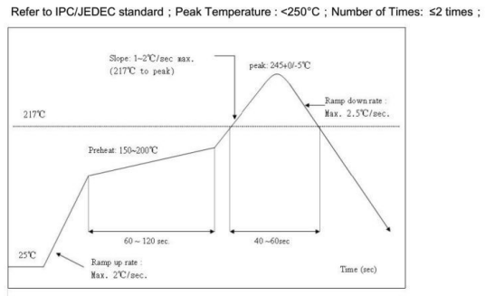
6.3 Recommended Oven Temperature Profile
TYWE3S Data Sheet
- 1. Product Overview
- 1.1 Features
- 1.2 Major application fields
- 2. Dimensions and Footprint
- 2.1 Dimensions
- 2.2 Definition of pin
- 2.3 Definition of test point
- 3. Electrical Characteristics
- 3.1 Absolute Electrical Characteristics
- 3.2 Electrical conditions
- 3.3 WI-Fi TX Power Consumption
- 3.4 WI-Fi RX Power Consumption
- 3.5 Power Consumption in Operating Mode
- 4. RF Features
- 4.1 Basic RF Features
- 4.2 WI-FI Output Power
- 4.3 RF RX sensitivity
- 5. Antenna Information
- 5.1 Antenna type
- 5.2 Antenna Interference Reduction
- 6. Packaging Information and Poduction Instructions
- 6.1 Mechanical Dimensions
- 6.2 Production Instructions
- 6.3 Recommended Oven Temperature Profile